
First tiny ASIC sent to manufacturing
 5 years ago making microchip from high-level HDL with your own hands required around 300k$ worth of software licenses, process was slow and learning curve steep.
Yesterday I've submitted my first silicon for manufacturing and it was... different. In the evening wife comes as asks "How much time until deadline?". I reply: "2 hours left, but I still have to learn Verilog." (historically my digital designs were in VHDL or schematic).
All this became possible thanks to Google Skywater PDK and openlane synthesis flow - which allowed anyone to design a microchip with no paperwork to sign and licenses to buy. Then https://tinytapeout.com by Matt Venn lowered the barrier even further (idea to tapeout in ~4 hours, including learning curve).
As expected, this all allows much more people to contribute to open source flow, with my favorite being work of Teodor-Dumitru Ene https://github.com/tdene) on hardware adders which now match and beat commercial tools. I think (and hope) that in 5 years opensource tools will dominate the market on mature nodes (28nm and up), not because they are cheaper, but because they are better and easier to use.
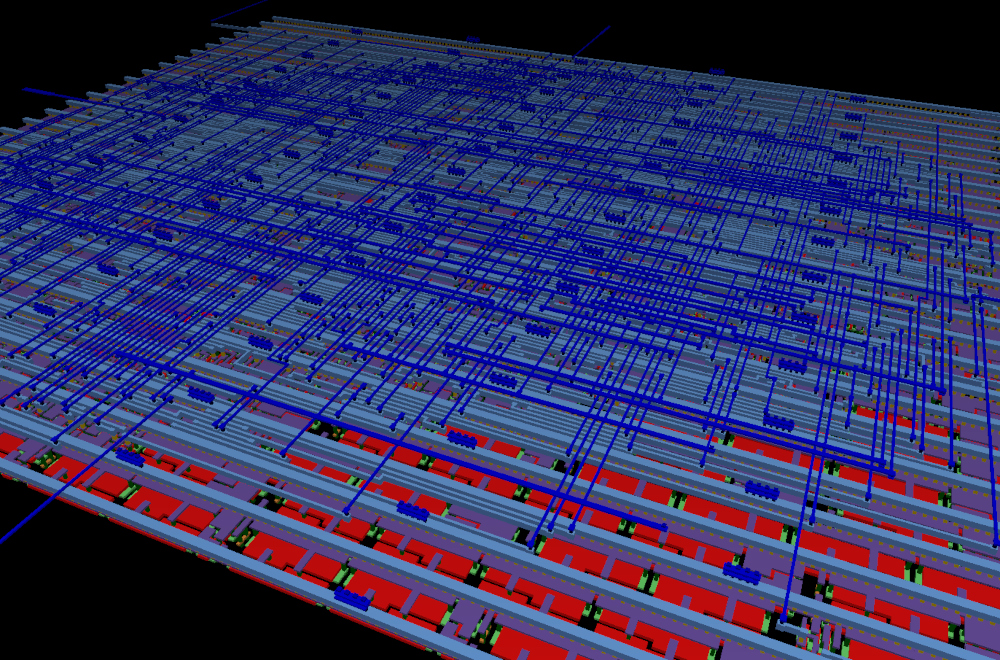
My design fits in 100x100µm and contains 289 standard cells. There are 7 ring oscillators with frequency dividers to compare silicon performance to analog simulation across voltage/temperature. I expect to see chips in ~6-9 months, both working and under microscope :-)


September 4, 2022

 @BarsMonster